|
|
| -Lead Pin | +Lead Pin | Vdc Minimum | Vdc Maximum |
|---|---|---|---|
| 4 4 |
1 2 |
+4.8 +4.8 |
+ 5.25 + 5.25 |
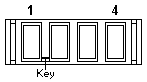
Connectors P2, P2A
| -Lead Pin | +Lead Pin | Vdc Minimum | Vdc Maximum |
|---|---|---|---|
| 4 4 |
1 2 |
+ 3.3 + 3.3 |
+ 5.25 + 5.25 |
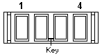
Connector P3
| -Lead Pin | +Lead Pin | Vdc Minimum | Vdc Maximum |
|---|---|---|---|
| 2 2 2 2 |
4 5 8 10 |
+11.52 +11.52 -10.8 + 4.8 |
+12.65 +12.65 -13.2 + 5.25 |
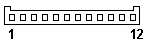
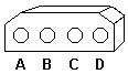
Connectors P4, P5, P6, P7, P8, P9 and P10
| -Lead Pin | +Lead Pin | Vdc Minimum | Vdc Maximum |
|---|---|---|---|
| B B |
A D |
+ 4.8 +11.52 |
+ 5.25 +12.6 |
Please see the LEGAL - Trademark notice.
Feel free - send a  for any BUG on this page found - Thank you.